HDD GURU FORUMS http://forum.hddguru.com/ |
|
Looking for in depth documentation on SSD PCB pins http://forum.hddguru.com/viewtopic.php?f=10&t=37647 |
Page 1 of 1 |
Author: | alpaca [ November 5th, 2018, 15:32 ] |
Post subject: | Looking for in depth documentation on SSD PCB pins |
Is there any documentation on the pin and solder pads like the ones e.g. at the bottom here: https://cdn.transcend-info.com/products ... MSA230.png This is just an example with lots of pins, I would be grateful for documentation on other models. |
Author: | HaQue [ November 5th, 2018, 21:48 ] |
Post subject: | Re: Looking for in depth documentation on SSD PCB pins |
you will have to do research. look at things like: -development boards for SSDs -Schematics for devices -
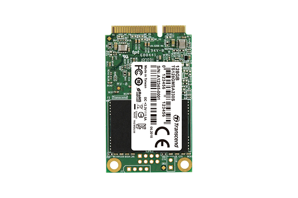
search for SSD images, look on the images for ports that are silkscreened labelled on the PCB, then match up the port pins configuration with the subject and see if you can tell by testing that is is the same kind of port. -use something like a JTAGulator to test possible JTAG ports -try seeing if you can get serial output on possible serial ports etc etc Attachment: Pp_MSA230.png [ 160.01 KiB | Viewed 7158 times ] |
Author: | alpaca [ November 6th, 2018, 6:50 ] |
Post subject: | Re: Looking for in depth documentation on SSD PCB pins |
Thanks. Do you have any ideas of the golden solder blobs. Like on the top leftor next to the firmware update port. There are also lots of solder blobs (test points?) on msata ssd I have.Is there maybe something common across the different models? |
Author: | fzabkar [ November 6th, 2018, 15:53 ] |
Post subject: | Re: Looking for in depth documentation on SSD PCB pins |
For an SM2246XT development kit, see viewtopic.php?f=10&t=35425 @sourcerer has done a great deal of reverse engineering work on a Samsung 840 Evo, including JTAG-ing. http://www2.futureware.at/~philipp/ssd/ http://www2.futureware.at/~philipp/ssd/TheMissingManual.pdf |
Author: | HaQue [ November 6th, 2018, 16:51 ] |
Post subject: | Re: Looking for in depth documentation on SSD PCB pins |
If you mean this, it is just some PCBs can be used for say 256GB or 512GB drives, or have different parts depending on different versions of chips used. Usually there are more locations for electronic parts than actual parts. The blobs are nothing special, just places where no parts were soldered. "unpopulated" Attachment:
|
Author: | fzabkar [ November 6th, 2018, 17:14 ] |
Post subject: | Re: Looking for in depth documentation on SSD PCB pins |
HaQue wrote: If you mean this, ... I think the OP is referring to the diamond shaped "pads" such as the one below "SW3". I haven't been involved in PCB manufacturing, so I may be wrong, but I suspect that these are registration points used for aligning multiple PCB layers. |
Page 1 of 1 | All times are UTC - 5 hours [ DST ] |
Powered by phpBB © 2000, 2002, 2005, 2007 phpBB Group http://www.phpbb.com/ |