It may be a Patriot brand with a Phison PS3109-S9-J controller.
Shorting R29 has no effect.
Thanks in advance,
Jon
| Attachments: |
|
IMG_3332.jpg [ 1.82 MiB | Viewed 8105 times ] |
|
IMG_3330.jpg [ 1.74 MiB | Viewed 8105 times ] |
| HDD GURU FORUMS http://forum.hddguru.com/ |
|
| Can anyone identify the shorting points for safe mode? http://forum.hddguru.com/viewtopic.php?f=10&t=38210 |
Page 1 of 1 |
| Author: | jono-ats [ March 17th, 2019, 16:40 ] | |||
| Post subject: | Can anyone identify the shorting points for safe mode? | |||
It may be a Patriot brand with a Phison PS3109-S9-J controller. Shorting R29 has no effect. Thanks in advance, Jon
|
||||
| Author: | fzabkar [ March 17th, 2019, 23:47 ] |
| Post subject: | Re: Can anyone identify the shorting points for safe mode? |
FWIW, here is an identical (?) PCB: MyDigitalSSD Super Cache 2 64GB Benchmarks and Review: https://www.servethehome.com/mydigitalssd-super-cache-2-64gb-benchmarks/ 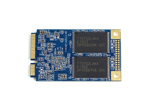 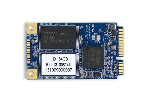 Is that a standard NAND pinout? If so, would it make sense to short the R/B* pin to ground? Did you measure the voltages at the "E3" inductors (L1 and L2) and "L7" polyfused (F1)? |
|
| Author: | jono-ats [ March 18th, 2019, 15:20 ] | ||
| Post subject: | Re: Can anyone identify the shorting points for safe mode? | ||
THANK YOU fzabkar. Got it through trial and error.
|
|||
| Author: | fzabkar [ March 18th, 2019, 16:51 ] |
| Post subject: | Re: Can anyone identify the shorting points for safe mode? |
Trial and error, in the absence of precautions, is a very dangerous approach. I saw those same two pads, but refrained from suggesting that you try shorting them. One of them appears to be connected to pin #7 (Ready/Busy*). However, the other pad could be connected to ground or Vcc, or somewhere else. NAND datasheets specify that R/B* is open drain. This means that the pin is driven to ground when the NAND is Busy, and allowed to float to Vcc when the NAND is Ready. Normally one would expect a pullup resistor on that pin, either as a discrete external component or an internal pullup within the flash controller (?). If those two pads are in fact reserved for a pullup, then your tweezers would be shorting the R/B* pin to Vcc. This could destroy that pin, especially if the NAND is trying to signal BUSY*. To avoid this possibility, I would have started by checking the voltages and connectivity of those pads to confirm that one is connected to R/B* and the other to ground. BTW, I wonder whether any of those pads at the edge of the PCB is connected to R/B*. If so, then it may prove useful for other similar SSDs. I also wonder whether shorting R/B* to ground could be a universal approach for all SSDs. |
|
| Author: | jono-ats [ March 19th, 2019, 11:40 ] |
| Post subject: | Re: Can anyone identify the shorting points for safe mode? |
I agree. It's a completely last resort. Thanks for the caveats. I wish I had time to do the research to satisfy your curiosity and other questions. However, there are so many dog recoveries to work in the queue on that I think I'm in a kennel club not a DR lab. |
|
| Author: | fzabkar [ March 19th, 2019, 16:54 ] |
| Post subject: | Re: Can anyone identify the shorting points for safe mode? |
There is no excuse for haphazard, dangerous, "last resort" techniques when dealing with a client's data. AISI, this case could have been solved with a logical, "first resort" approach. At the very least I would expect that professionals should take the time to learn something about electronics before playing with it. You owe it to your customers. I have seen numerous "trial and error" threads that make me cringe. For example, one prominent forum member intentionally reversed the power supply connections to an unknown NAND after his initial attempt failed to detect it. The correct solution in such cases is to examine the PCB and note the connectivity of the NAND's bypass capacitors, then, if possible, measure the capacitor voltages. Another horror story was when another prominent forum member soldered an unknown NAND, with a non-standard package, onto a regular ONFI jig, with the result that supply rails were wired to data pins. As before, the proper approach would have been to refer to the PCB and determine the NAND's pinout with reference to its controller and adjacent capacitors. But that requires time and effort ... It appears that the solution in the present case was to short the R/B* (Ready/Busy*) pin to ground. This pin is "open drain" and is designed to be switched directly to ground (as are "open collector" pins). Therefore, all one needs to do is to locate, with a DMM or by visual inspection, a test point which connects to pin #7 (R/B* for a standard ONFI NAND). One can then safely short this test point to ground. https://en.wikipedia.org/wiki/Open_collector When the NAND is in the Busy state, its open drain (or open collector) output is driven to ground via a transistor switch. Conversely, when the NAND is in the Ready state, this same switch is open. Code: open collector open drain VCC VCC VCC + + + | | | | | | .-. pullup .-. pullup .-. pullup | | resistor | | resistor | | resistor | | | | | | '-' '-' '-' Ready/Busy* | Ready/Busy* | Ready/Busy* | o o o .--------|--. .--------|--. .--------|--. | C| | | D| | | | | | | | | | | | | | | |/ | | |-+ | | | | | B -| | NPN | G | | N-channel | \ | | |> | BJT | ->|-+ | JFET | \ | | | | | | | | switch | | | E| | | S| | | | | '--------|--' '--------|--' '--------|--' NAND | NAND | NAND | === === === GND GND GND B = base G = gate off = Ready C = collector D = drain on = Busy* E = emitter S = source As you can see, if you were to short the two ends of the external pullup resistor, and if the NAND were in the Busy state, you would be connecting Vcc directly to ground via the closed switch. This could seriously damage, or destroy, the switch. |
|
| Author: | jono-ats [ March 20th, 2019, 10:40 ] |
| Post subject: | Re: Can anyone identify the shorting points for safe mode? |
Thanks for your pompous lecture. Interesting coming from a guy who claims he doesn't do data recovery . . . BTW, we didn't damage the chip and are reading data from it. I have never damaged a client's SSD. |
|
| Author: | fzabkar [ March 20th, 2019, 18:37 ] |
| Post subject: | Re: Can anyone identify the shorting points for safe mode? |
jono-ats wrote: Thanks for your pompous lecture. Interesting coming from a guy who claims he doesn't do data recovery . . . BTW, we didn't damage the chip and are reading data from it. I have never damaged a client's SSD. Your clients deserve due diligence. This means that you should not poke about randomly with tweezers on their live data. The user in this thread was not so lucky: http://www.hddoracle.com/viewtopic.php?f=3&t=1983 He damaged one of the boot configuration pins on his Marvell MCU by shorting it to Vcc. Unlike you, he did not do this haphazardly. Instead he followed the shorting instructions that came with the DR software he was using (U-Command). We verified the damage by measuring the resistance looking into that particular pin. Strangely, the damage was not immediate -- after his first few attempts he was able to access BOOT ROM mode, or whatever it is called. Subsequent attempts failed. That's when we noticed the damaged pin. Peeking at this pin via the corresponding port in the ROM monitor confirmed that it was "stuck". |
|
| Page 1 of 1 | All times are UTC - 5 hours [ DST ] |
| Powered by phpBB © 2000, 2002, 2005, 2007 phpBB Group http://www.phpbb.com/ |
|