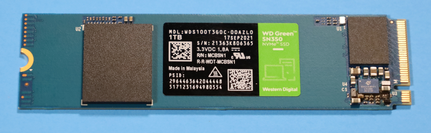
All times are UTC - 5 hours [ DST ]


Post new topic Reply to topic  [ 6 posts ] 
Author Message
 Post subject: WD Green SSD with burnt components at power input
PostPosted: April 27th, 2023, 10:19 
Offline

Joined: August 26th, 2021, 17:52
Posts: 61
Location: Brasil
Hello everyone!

This week, one of my clients gave me a WD Green SSD, model sn350. Two components located at the power input, a zener diode and a 6-pad BGA IC, had burned out. I assume that the IC had the function of waiting for the power to stabilize before activating the PMIC. I am attaching a photo of the board focused on the power input area after removing both the zener diode and the IC. For clarity, I have marked their positions with colored rectangles. The zener diode was in the yellow rectangle and the IC in the red one.

Using a multimeter, I measured the continuity between the two pads on the left of the IC, which I numbered as 1 and 2, with the top left end of the capacitor. The two center pads and the bottom left pad, numbered 3, 4, and 6, receive 3.3v directly from the input. The only pad I couldn't identify is number 6.

Since I don't have a donor to replace the burned components, I am thinking of joining pads 1 and 2 with pads 3 and 4 to solve the problem, but before doing so, I would like to consult whether it is a good idea.

I am also attaching a photo of the BGA IC. I tried to look up the codes written on the package on the Texas Instruments website (https://www.ti.com/packaging/docs/partl ... sp#divline), but without success. The IC have 2 code parts written 17A6YCI and 28203.


Thanks very much and my best regards to all, thanks to read


Attachments:
IMG_20230425_193006100.jpg
IMG_20230425_193006100.jpg [ 51.46 KiB | Viewed 2167 times ]
ssd.png
ssd.png [ 535.59 KiB | Viewed 2167 times ]
Top
 Profile  
 
 Post subject: Re: WD Green SSD with burnt components at power input
PostPosted: April 27th, 2023, 13:30 
Offline
User avatar

Joined: September 8th, 2009, 18:21
Posts: 15538
Location: Australia
Pin #1 is the large dot. Pins are numbered anticlockwise. You have mentioned pin #6 twice. Did you mean pin #5 the second time?

Is pin #5 connected to DEVSLP on the interface?

This PCB has an "AF" or "RF" part in the same place:

https://www.servethehome.com/wp-content/uploads/2022/03/WD-Green-SN350-1TB-Front.jpg

The diode would be a TVS diode rather than a zener. (A TVS diode is much faster than a zener.)

I expect that U3 is a switch of some kind, eg MOSFET, load switch, e-fuse.

Try to identify the date codes on the major ICs. That should help to identify the date codes on U3.

Do your 1 and 2 pins connect to more than I capacitor? If so, then this would suggest that it is a 3.3V output from the IC rather than an output from an LDO regulator.

_________________
A backup a day keeps DR away.


Top
 Profile  
 
 Post subject: Re: WD Green SSD with burnt components at power input
PostPosted: April 27th, 2023, 13:50 
Offline
User avatar

Joined: September 8th, 2009, 18:21
Posts: 15538
Location: Australia
The fact that U3 does not have a ground pin (?) suggests that it is a MOSFET.

The alternative part is marked "AF":

https://images.mltrade.ru/images/photo/n/x/a/579443-078088-4.webp

_________________
A backup a day keeps DR away.


Top
 Profile  
 
 Post subject: Re: WD Green SSD with burnt components at power input
PostPosted: April 27th, 2023, 14:09 
Offline
User avatar

Joined: September 8th, 2009, 18:21
Posts: 15538
Location: Australia
PMCM6501UPE, P-channel enhancement mode MOSFET, -20V, -7.3A, Nexperia, marking AF, WLCSP6:
https://assets.nexperia.com/documents/data-sheet/PMCM6501UPE.pdf

You should be able to bridge the drain and source pins. However, I would first confirm that there are no shorts at the inputs and outputs of the PMIC.


Attachments:
PMCM6501UPE_pinout_symbol.gif
PMCM6501UPE_pinout_symbol.gif [ 42.04 KiB | Viewed 2122 times ]

_________________
A backup a day keeps DR away.
Top
 Profile  
 
 Post subject: Re: WD Green SSD with burnt components at power input
PostPosted: April 27th, 2023, 15:03 
Offline

Joined: August 26th, 2021, 17:52
Posts: 61
Location: Brasil
fzabkar wrote:
PMCM6501UPE, P-channel enhancement mode MOSFET, -20V, -7.3A, Nexperia, marking AF, WLCSP6:
https://assets.nexperia.com/documents/data-sheet/PMCM6501UPE.pdf

You should be able to bridge the drain and source pins. However, I would first confirm that there are no shorts at the inputs and outputs of the PMIC.


FZABKAR THANKS VERY MUCH, I AM VERY GRATEFUL FOR YOUR HELP

SOON I WILL DO TESTS


Top
 Profile  
 
 Post subject: Re: WD Green SSD with burnt components at power input
PostPosted: April 29th, 2023, 10:07 
Offline

Joined: August 26th, 2021, 17:52
Posts: 61
Location: Brasil
Hello everyone!

I am able to recover the data doing a short circuit between the pads of SOURCE and DRAIN.

Thanks very much, FZABKAR


Top
 Profile  
 
Display posts from previous:  Sort by  
Post new topic Reply to topic  [ 6 posts ] 

All times are UTC - 5 hours [ DST ]


Who is online

Users browsing this forum: aumax, Tawfeek and 100 guests


You cannot post new topics in this forum
You cannot reply to topics in this forum
You cannot edit your posts in this forum
You cannot delete your posts in this forum
You cannot post attachments in this forum

Search for:
Jump to:  
Powered by phpBB © 2000, 2002, 2005, 2007 phpBB Group