Forum rules
Please do not post questions about data recovery cases here (use this forum instead). This forum is for topics on finding new ways to recover data. Accessing firmware, writing programs, reading bits off the platter, recovering data from dust...Re: Marvell 88i6745n JTAG
August 31st, 2011, 12:17
it's pretty basic for PDA and phone phreaks 
Re: Marvell 88i6745n JTAG
August 31st, 2011, 18:14
About "Kernel Loader"
First we have to know somethig about kernel blocks in flash.
They have 0x20 bytes headers like first one for kernel loader.
;-------------------------------------
1 ;block nr
1 ;describe typ? 1,3 = compresed data?
0,0 ;maybe high 16 bits of decompresed size?
0x51,0x70,0,0 ;=0x00007051 size of block with CHK
0x50,0x70,0,0 ;=0x00007051 size of block
0x2d,0xd,0,0 ;=0x00000d2d offset of block data in FLASH (physical addr 0xfff00d2d)
0,0,0,0 ;=0x00000000 physical addr where decompresed block have to be stored
0xff,0xff,0xff,0xff ;=0xffffffff execute address but if it is 0xffffffff then it will not be executed!
1,0xa,0,0 ;?
0x48,0x8c ;=0x8c48 lower 16 bits of decompresed size.
0 ;?
0x98 ;cheksum
;-------------------------------------
Once started, "Kernel Loader" initialize SDRAM, change vector base,etc.
Then it test block header, copy block to sdram, decompres from sdram to appropriate destination.
if "execute address" is 0xffffffff then next block will be handled.
Once "execute address" is not 0xffffffff,kernel loader will execute code from that address.
In my case it is 0x00000000, reset vector!!!
If any of blocks have bad data cheksum, "kernel loader" will loop( It is related to SATA communication)
In my case one of kernal block was demaged, and I found a way to repair using JTAG debugger.
This will work only if you already have correct backup, and "flash loader" is not corupted.
(If your "flash loader" is also corupted then procedure is a little different)
Get dump of FLASH data using JTAG, and compare with previous backup to find what block is demaged (look to block headers description in this post).
Create file of that blocks from backup file using some hexeditor.
Set your board to test mode(first three pins from jumper header connect to GND)
Connect JTAG, SATA cable and power up board.
Run JTAG debugger.
Halt target.
Look to "offset address" of demaged block and add 0xfff00000 to get phisical address.
Use that address to set in debuger watch point with read mode only.
Set PC to 0xffff0000
AND HIT RUN!!!
If everything is ok it will halt CPU. Look at dissasembled code in debugger to find
what is destination address in "copy_mem" function. Now set break point on end of that
rutine.
Hit RUN again.
Once halted load data from file that you previously created to destination address, to
owerwrite bad data from flash.
Repeat this to every block that is corrupted.
Finaly just hit RUN and drive will start to communicate over SATA.
Now you can use free program "WDR-demo" to write backup FLASH to board.
And that is it!
Now since I repaired my drive I can look for rutine for writing FLASH.
B.R
Dejan
Re: Marvell 88i6745n JTAG
September 2nd, 2011, 6:14
http://icegsm.narod.ru/Programms.htm
EJTAG_TT
The program is a JTAG programming of flash. Originally conceived for flashing receivers, but can be used not only for them.
Currently supported processors are the following (in absolute value):
1. Ali M3327, 29
At the moment the only program that allows receivers to flash with the processor and the SPI-flush. Applied a special algorithm for fast programming of flash data to the processors based on MIPS-optimized commands.
Forum thread
2. NEC EMMA2L (L) (uPD6111h)
The basis was taken EJFlasher, redesigned and much improved as a result of the speed of these processors. Supports the new processor NEC EMMA2SL (uPD61217), reaching a new receivers Interstar XPEED.
Forum thread
3. ARM7 / 9
This module was developed in the program for flashing receivers processor-based Conexant CX24138-43. You can use for other ARM processors (tested on ARM7TDMI AD6522 - LG-5200).
Twig Forum Conexant
4. It supports multiple MIPS-processor, such as Broadcom, BRECIS etc
5. Processors ST20 (module is enabled only for beta testers).
Currently it supports the processor STI 5518. The module will be activated in a future release (after testing STI 5119).
Re: Marvell 88i6745n JTAG
September 2nd, 2011, 10:04
please, Replace picture on the post.
- Attachments
-
Re: Marvell 88i6745n JTAG
September 2nd, 2011, 12:02

Re: Marvell 88i6745n JTAG
September 2nd, 2011, 17:44
Ok. I found rutine for writing internal FLASH.
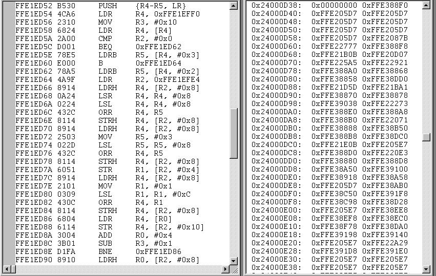
On right side is Main Command table so you can find other commands.
On left side is rutine that writes 0x40 bytes to internal flash.
Base port for FLASH is 0x1c00aa00
[0x1c00aa08] and 0xff00 or 7
[0x1c00aa08] or 300h
[0x1c00aa04] <= 32 bit addres to write in FLASH
[0x1c00aa08] or 1000h
[0x1c00aa10] <= [32 bit data]++ * 0x10 ;writing 0x10 32it data to flash
[0x1c00aa08] and not 1000h
etc,etc.......
NOW YOU HAVE EVERYTHING TO MAKE PROGRAM TO REPAIR FLASH USING SERIAL COMUNICATION!
B.R.
Dejan
- Attachments
-
Re: Marvell 88i6745n JTAG
September 2nd, 2011, 19:16
Nice work
You are one of the fastest reversers I've ever seen
I'm not familiar with this CPU flash commands, is it one flash bank or several?
Did you find how to switch between banks?
You are one of the fastest reversers I've ever seen
I'm not familiar with this CPU flash commands, is it one flash bank or several?
Did you find how to switch between banks?
Re: Marvell 88i6745n JTAG
September 3rd, 2011, 4:35
Dejan,
I guess by looking @ your post here about this issue you are familiar with the SoftICE right?
really interesting post
I guess by looking @ your post here about this issue you are familiar with the SoftICE right?
really interesting post
Re: Marvell 88i6745n JTAG
September 4th, 2011, 10:09
Excellent thread!
I've been trying to access rom on a 2061-701450 board without luck...
Did you populate r21 (jtag_sel?)
Anyway you did a great job!
I've been trying to access rom on a 2061-701450 board without luck...
Did you populate r21 (jtag_sel?)
Anyway you did a great job!
Re: Marvell 88i6745n JTAG
September 4th, 2011, 10:56
viktdev wrote:Excellent thread!
I've been trying to access rom on a 2061-701450 board without luck...
Did you populate r21 (jtag_sel?)
Anyway you did a great job!
I tested on 2061-701335-c00 Marvell 88i6545 and 2061-701499-e00 Marvell 88i6745n,
and I don't populate any resistor on those boards.
Re: Marvell 88i6745n JTAG
September 4th, 2011, 11:02
einstein9 wrote:Dejan,
I guess by looking @ your post here about this issue you are familiar with the SoftICE right?
really interesting post
I don't know that SoftICE can debugg ARM cores?
You can use any JTAG ARM Debugger, WinARM, Ti CCS, NoICE, KEIL, etc,etc...
Re: Marvell 88i6745n JTAG
September 4th, 2011, 11:09
Doomer wrote:Nice work
You are one of the fastest reversers I've ever seen
I'm not familiar with this CPU flash commands, is it one flash bank or several?
Did you find how to switch between banks?
What banks?
Internal EEPROM or FLASH have only 192k and is fully maped in space 0xfff00000
Internal EEPROM or FLASH when write have page in size of 0x40
Re: Marvell 88i6745n JTAG
September 4th, 2011, 11:32
_dex_ wrote:What banks?
Flash banks
_dex_ wrote:Internal EEPROM or FLASH have only 192k and is fully maped in space 0xfff00000
correction
it CAN be mapped.
It depends in which boot mode you start a drive
The mapping supposed to be enabled and one of the boot modes does that
Re: Marvell 88i6745n JTAG
September 4th, 2011, 12:28
Doomer wrote:_dex_ wrote:What banks?
Flash banks_dex_ wrote:Internal EEPROM or FLASH have only 192k and is fully maped in space 0xfff00000
correction
it CAN be mapped.
It depends in which boot mode you start a drive
The mapping supposed to be enabled and one of the boot modes does that
Your posts are totaly strange.
Where I did wrote that it can NOT be mapped?
FLASH banks are used in case when size of flash are bigger than address space.
In that case size of FLASH are divided into blocks(banks) that are selected by HW.
In this case address space is 32bit and size of FLASH is 18bit.
About mapping.
Every ARM CPU have paging any you can remap every port, memory.
Mapping alows to change physical address of some port,mem
and/or to allows multiple images of same port,mem
Re: Marvell 88i6745n JTAG
September 4th, 2011, 13:39
I'm just trying to find out how the things really work
That's it
The reason why I'm asking about flash banks is that if address reg is 32 bits doesn't mean that flash address uses 32 or even 18 bits inside. If there is no banks then there is no banks
This is interesting discussion and if you found how to program flash from the beginning (chip select, unprotect, erase etc.) I would like to discuss it
But I understand if you don't want it
I better shut up
Re: Marvell 88i6745n JTAG
September 6th, 2011, 15:00
Why you are making it so complicated ?? do you have pc3000 ?
Re: Marvell 88i6745n JTAG
September 6th, 2011, 15:03
Why you are making it so complicated?? Do you have pc3000 & donor drive or similar PCB ?
Re: Marvell 88i6745n JTAG
September 6th, 2011, 17:48
Farhan709 wrote:Why you are making it so complicated?? Do you have pc3000 & donor drive or similar PCB ?
I don't think you understand this at all, how do you use pc3000 on a wrongly flashed marvell chip or a dead pcb?
Re: Marvell 88i6745n JTAG
September 7th, 2011, 0:38
_dex_ wrote:einstein9 wrote:Dejan,
I guess by looking @ your post here about this issue you are familiar with the SoftICE right?
really interesting post
I don't know that SoftICE can debugg ARM cores?
You can use any JTAG ARM Debugger, WinARM, Ti CCS, NoICE, KEIL, etc,etc...
Dejan,
After Squeezing my Memory for a very long time, I REMEMBER NOW
but seems YOU FORGOT REALLY
We Have done some Biz. long time back, and i mean here long (more than 6-7y)
Am looking @ my old Archived MailBox (hope i can find it) and will extract some discussions info. from there which we had long time back by emails and will get back to you here and PM once i find it
Really, NICE TO SEE YOU HERE AGAIN, As they said: Life Circulate.
Re: Marvell 88i6745n JTAG
September 7th, 2011, 16:19
Doomer wrote:I'm just trying to find out how the things really work
That's it
The reason why I'm asking about flash banks is that if address reg is 32 bits doesn't mean that flash address uses 32 or even 18 bits inside. If there is no banks then there is no banks
This is interesting discussion and if you found how to program flash from the beginning (chip select, unprotect, erase etc.) I would like to discuss it
But I understand if you don't want it
I better shut up
Well, I allready told you that I repaired FLASH using JTAG debugger. I did not analyze much
how rutines for writing works but it is not complicated. You have to trace program using JTAG.
Powered by phpBB © phpBB Group.