I talked to customer to get more infos about how the pcb got damaged.
He said that native pcb just did smoke while the drive was working, after that drive didn't work anymore.
So he bought donor PCB (which is the one you see in posted pics) and he tried to do IC2 chip swap with his hotair soldering station, it didn't work so he decided to unsolder it again.
The chip you see on pic it's from native PCB!
I look carefully IC2 chip under microscope, i found that some pins were bended and few pads on board where shorted by welding residues, probably this explains why his "repair job" didn't work.
I have also found that one of those 2 fuse near top left corner is opened, very likely because he powered on the drive with shorted IC2 pins or because he had not placed it properly on board.
Attachment:
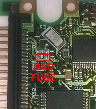 Fuse.JPG [ 27.41 KiB | Viewed 12776 times ]
Now i have removed welding residues from IC2 pads and very carefully straightened chip pins under microscope with the tip of a small screwdriver.
Tomorrow i will try to find a similar fuse to replace the bad one.
fzabkar wrote:
I'm not certain, but the motor controller at the top left appears to be associated with transistors Q3, Q4, Q13 and a fourth transistor below Q13. I don't know whether these transistors are regulators or motor drivers, but I would measure their voltages before I would replace IC2.
IC2 at the moment is out of the board, should i measure those voltages now or after i will soldered it on pcb?