Page 1 of 2
SK Hynix SC308 hfs256g39tnd-n210 need a component name
Posted: May 12th, 2020, 3:21
by sandro123
Please help me for find this component or any info.
Micro bga 6 ball
Enter a 3,3V and out 0V
Thank you for any info

- ck.JPG (48.02 KiB) Viewed 25620 times
Sandro
Re: SK Hynix SC308 hfs256g39tnd-n210 need a component name
Posted: May 12th, 2020, 3:38
by fzabkar
Could we see the whole PCB? Sometimes it is easier to identify the IC when it is viewed in the context of its surroundings.
Re: SK Hynix SC308 hfs256g39tnd-n210 need a component name
Posted: May 12th, 2020, 4:04
by fzabkar
I suspect that the part may be a load switch or a P-channel MOSFET, probably controlled from the DevSlp input.
Re: SK Hynix SC308 hfs256g39tnd-n210 need a component name
Posted: May 12th, 2020, 4:29
by fzabkar
It's not the correct part, but it could be something like this:
https://www.onsemi.com/pub/Collateral/FPF1039-D.pdf
Re: SK Hynix SC308 hfs256g39tnd-n210 need a component name
Posted: May 12th, 2020, 5:06
by sandro123
Thank for this help.
check all boards, used in Kingston and Hinix.
I think is this component, try to confirm pinout whit DEVSLP pin.
thanks!
Re: SK Hynix SC308 hfs256g39tnd-n210 need a component name
Posted: May 12th, 2020, 16:41
by fzabkar
If this IC is the main load switch, then its On/Off pin should be controlled via DevSlp (pin #38).
http://www.hddoracle.com/download/file.php?id=7418&mode=viewThe Vout pin should connect to the Vcc pins of the DC-DC converters. You photo is too poor, but I managed to find a clearer photo with Google. AFAICT, two of the regulators are marked with "AZ".
MP2162, Monolithic Power, Synchronous Step-Down Converter, marking AZ, 2A, 6V, 1.5MHz, QFN-8:
https://www.monolithicpower.com/pub/media/document/MP2162_r1.03.pdf
Re: SK Hynix SC308 hfs256g39tnd-n210 need a component name
Posted: May 14th, 2020, 3:21
by fzabkar
In this photo, the chip looks more like a fixed LDO regulator:
https://cdn.mos.cms.futurecdn.net/LDpLp4YTVFL5bxYr577MeE-1182-80.pngThe small black square devices near the AZ parts appear to be load switches for standby mode.
Re: SK Hynix SC308 hfs256g39tnd-n210 need a component name
Posted: May 14th, 2020, 3:42
by fzabkar
Re: SK Hynix SC308 hfs256g39tnd-n210 need a component name
Posted: May 14th, 2020, 7:04
by BrandonMllr
there was a similar problem, I still did not figure it out ..
Re: SK Hynix SC308 hfs256g39tnd-n210 need a component name
Posted: May 15th, 2020, 16:13
by fzabkar
BrandonMllr wrote:there was a similar problem, I still did not figure it out ..
It's simple enough.
If the IC is a load switch (which I now doubt), then run a wire link from Vin to Vout. DO NOT do this unless you are certain that this is indeed the function of the IC..
If the IC is an LDO regulator (which I now believe), then replace it with any suitable LDO with the correct Vout. For example, if Vout =1.8V, then you could substitute an LM1117-1.8.
One thing that needs to be confirmed is whether there is a short between Vout and ground, in which case I would suspect a bad controller or bypass capacitor.
Re: SK Hynix SC308 hfs256g39tnd-n210 need a component name
Posted: February 4th, 2022, 6:39
by DeVlL
Hello.
I take advantage of the thread, because I have exactly the same unit.
I attach detailed photos.
Full Photo:
https://i.ibb.co/XxV83PD/HFS256-G39-TND-N210-A-Full.jpgDetailed photo:
https://i.ibb.co/80s1VPz/HFS256-G39-TND-N210-A-1-2.jpghttps://i.ibb.co/mtJwhD2/HFS256-G39-TND-N210-A-2-2.jpgSistomas: The unit when connected does not show any signs of life. The bios does not detect it and as is logical neither windows nor linux, it has been left connected for about half an hour and no chip heats up.
I have looked at the voltage that it gives me in the same components that the creator of this thread puts and it gives me exactly the same as he did. I have checked the capacitors and the two input diodes and everything is correct.
What else can I check?
Does anyone know how to put this unit in safe mode?
Greetings and thanks for the help.
Re: SK Hynix SC308 hfs256g39tnd-n210 need a component name
Posted: February 4th, 2022, 15:19
by fzabkar
@DeVlL, what are the markings on the first IC at the bottom left ("CK PJ" in first photo)?
What are the markings on IC1 - 5? I suspect that IC1 - 3 are load switches, but I'm not sure about IC4.
Can you measure the voltages at Vin, Va, Vb, Vc, Va(sw), Vb(sw1), Vb(sw2)?
What are the voltages at the Enable pins for each IC?
Does the output of the first "CK PJ" IC connect to Vin?
Does the 3.3V input of the first "CK PJ" IC connect to Vin?
Re: SK Hynix SC308 hfs256g39tnd-n210 need a component name
Posted: February 8th, 2022, 9:18
by DeVlL
fzabkar wrote:@DeVlL, what are the markings on the first IC at the bottom left ("CK PJ" in first photo)?
What are the markings on IC1 - 5? I suspect that IC1 - 3 are load switches, but I'm not sure about IC4.
Can you measure the voltages at Vin, Va, Vb, Vc, Va(sw), Vb(sw1), Vb(sw2)?
What are the voltages at the Enable pins for each IC?
Does the output of the first "CK PJ" IC connect to Vin?
Does the 3.3V input of the first "CK PJ" IC connect to Vin?
Thanks for your help.
Here are your answers to your questions.
what are the markings on the first IC at the bottom left ("CK PJ" in first photo)?
It's a CK QP
Can you measure the voltages at Vin, Va, Vb, Vc, Va(sw), Vb(sw1), Vb(sw2)?
They all give me 0 voltage
What are the voltages at the Enable pins for each IC?
They also give me 0v voltage
Does the output of the first "CK PJ" IC connect to Vin?
The CK QP is connected to VIN
Does the 3.3V input of the first "CK PJ" IC connect to Vin?[/quote]
THE CK QP gives me 0v
I think the solution is in the input.
Here I show you the measurements at the entrance.
My question is. Could it be that the Rom bios is corrupt and there is no voltage for it to start? And from there my previous question. Does anyone know how to put this unit in safe mode?
Thanks
Re: SK Hynix SC308 hfs256g39tnd-n210 need a component name
Posted: February 8th, 2022, 13:50
by fzabkar
DeVlL wrote:It's a CK QP
That means that "CK" is the part number and PJ/QP are date or batch codes.
DeVlL wrote:Can you measure the voltages at Vin, Va, Vb, Vc, Va(sw), Vb(sw1), Vb(sw2)?
They all give me 0 voltage
What are the voltages at the Enable pins for each IC?
They also give me 0v voltage
I presume that Vin = 0V? If so, then the "CK" component must be the main switch, possibly a load switch or electronic fuse.
DeVlL wrote:Does the output of the first "CK PJ" IC connect to Vin?
The CK QP is connected to VIN
Does the 3.3V input of the first "CK PJ" IC connect to Vin?
THE CK QP gives me 0v
I presume you mean that the Vin test points are connected to the 0V output of the "CK" chip?
DeVlL wrote:I think the solution is in the input.
Here I show you the measurements at the entrance.
It does appear that "CK" is the main switch. My question is, is this switch being switched on? There should be a DevSlp pin on the m.2 interface (pin #38). Does it connect to the diode in the middle of the PCB, or does it connect to the "CK" chip?
http://www.hddoracle.com/download/file.php?id=7418&mode=viewhttp://www.hddoracle.com/viewtopic.php?f=106&t=2506DeVlL wrote:Could it be that the Rom bios is corrupt and there is no voltage for it to start?
That doesn't make sense. The two MP2162 ICs produce the Vcore and Vio supplies for the flash controller. If there is no voltage, then what does it matter if anything is corrupt?
DeVlL wrote:Does anyone know how to put this unit in safe mode?
Why?
My approach would be to determine the pinout of "CK". If the output of this chip is not shorted to ground, and if it is indeed a switch or e-fuse, then it should be OK to jumper its input and output.
If you can tell us the markings on ICs 1 - 5, then we may be able to identify them and their manufacturer. This might make it easier to identify "CK".
Re: SK Hynix SC308 hfs256g39tnd-n210 need a component name
Posted: February 8th, 2022, 15:01
by fzabkar
Can you confirm if this is the pinout of "CK"?
- Code:
+3.3V in   O  O   output
+3.3V in   O  O   output
+3.3V in   O  O   ground
Can you measure the resistance between the outputs and ground?
Can you confirm the connectivity of the m.2 DevSleep pin?
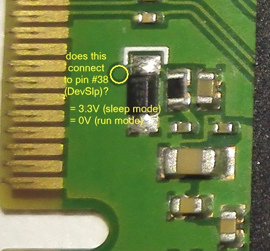
- DevSlp.jpg (187.4 KiB) Viewed 18580 times
Re: SK Hynix SC308 hfs256g39tnd-n210 need a component name
Posted: February 9th, 2022, 7:52
by DeVlL
fzabkar wrote:Can you confirm if this is the pinout of "CK"?
- Code:
+3.3V in   O  O   output
+3.3V in   O  O   output
+3.3V in   O  O   ground
Can you measure the resistance between the outputs and ground?
Can you confirm the connectivity of the m.2 DevSleep pin?
The attachment DevSlp.jpg is no longer available
I think the culprit is definitely CK QP.
Here I detail what you ask for and the conclusions that I believe the fault is in the CK QP:
Can you measure the resistance between the outputs and ground?
The measurements give completely crazy values, they go up and down. It is not a fixed value.
Can you confirm the connectivity of the m.2 DevSleep pin?
If there is connectivity to pin 38 DevSleep.
Now I attach an image of the CK QP. As you can see in the image the CK QP has a broken corner (I hadn't seen it because I don't have a microscope) I remembered that I had saved a USB microscope here and that is the image you see now.
In the second image with the measurements, it confirms that the possible failure is the CK QP. What do you think?
In a while I'll edit the message and tell you exactly the ICs from 1 to 5
Re: SK Hynix SC308 hfs256g39tnd-n210 need a component name
Posted: February 9th, 2022, 15:16
by fzabkar
Your measurements would suggest that there is no short between 3.3Vout and Ground. Your measurements would also suggest that 3.3Vout in connected to Vin(3.3V).
If this is correct, then it should be safe to connect a jumper wire between 3.3Vout and 3.3Vin.
Re: SK Hynix SC308 hfs256g39tnd-n210 need a component name
Posted: February 9th, 2022, 16:09
by fzabkar
For the benefit of others, here are my guesses as to suitable equivalents for IC1 - 3, and IC4.
SiP32462DB-T2-GE1, Vishay Siliconix, 50 mOhm, Slew Rate Controlled Load Switch, Vin = 1.2V - 5.5V, 1.2A, marking AH, WCSP4:
https://www.vishay.com/docs/67754/sip32461.pdfSiP32458, SiP32459, Vishay Siliconix, 20 mOhm, Slew Rate Controlled Load Switch, Vin = 1.5V - 5.5V, 3A, marking AA or AB, WCSP6:
https://www.vishay.com/docs/63999/sip32458.pdfThis appears to be IC5:
MP6400DG, Low Quiescent Current Programmable-Delay Supervisory Circuit, marking 5B, QFN6:
https://www.monolithicpower.com/pub/media/document/MP6400_r1.1.pdf
Re: SK Hynix SC308 hfs256g39tnd-n210 need a component name
Posted: February 10th, 2022, 5:58
by DeVlL
fzabkar wrote:For the benefit of others, here are my guesses as to suitable equivalents for IC1 - 3, and IC4.
SiP32462DB-T2-GE1, Vishay Siliconix, 50 mOhm, Slew Rate Controlled Load Switch, Vin = 1.2V - 5.5V, 1.2A, marking AH, WCSP4:
https://www.vishay.com/docs/67754/sip32461.pdfSiP32458, SiP32459, Vishay Siliconix, 20 mOhm, Slew Rate Controlled Load Switch, Vin = 1.5V - 5.5V, 3A, marking AA or AB, WCSP6:
https://www.vishay.com/docs/63999/sip32458.pdfThis appears to be IC5:
MP6400DG, Low Quiescent Current Programmable-Delay Supervisory Circuit, marking 5B, QFN6:
https://www.monolithicpower.com/pub/media/document/MP6400_r1.1.pdf
Here you have pictures of the ICs from 1 to 5
Re: SK Hynix SC308 hfs256g39tnd-n210 need a component name
Posted: February 10th, 2022, 6:03
by DeVlL
fzabkar wrote:Your measurements would suggest that there is no short between 3.3Vout and Ground. Your measurements would also suggest that 3.3Vout in connected to Vin(3.3V).
If this is correct, then it should be safe to connect a jumper wire between 3.3Vout and 3.3Vin.
So if I put a cable between those two points, in theory the bios/windows should detect it.
So is it a fuse?