Hello,
I try to recover data from broken USB stick for a friend. It's the first time I try to do that.
The USB stick is build around PS2251-09-26 and a "noname" NAND.
Attachment:
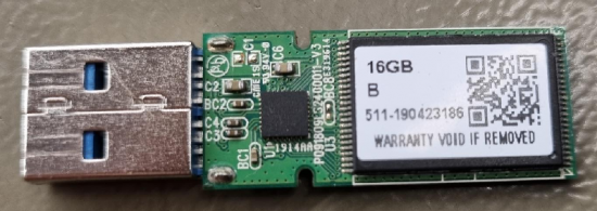 stick1.png [ 302.72 KiB | Viewed 12266 times ]
Attachment:
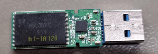 stick2.png [ 252.17 KiB | Viewed 12266 times ]
Controller PS2251-09-26 seem completely broken so I unsold carrefully the NAND
Attachment:
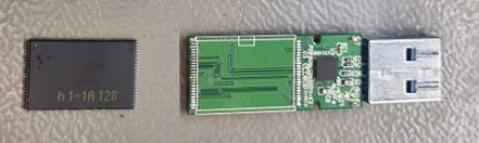 stick3.png [ 71.16 KiB | Viewed 12266 times ]
And I build a "Poor Man NAND Reader" with a TSOP48 adapter, a NUCLEO board and some dupont wires...
(I add a FT232H breakout to increase serial output speed).
Attachment:
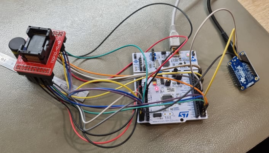 setup1.png [ 406.63 KiB | Viewed 12266 times ]
I write a peace of code to download data on PC from serial port.
Attachment:
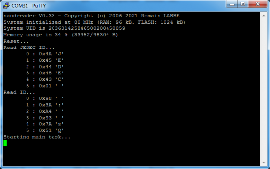 screen1.png [ 32.53 KiB | Viewed 12266 times ]
I'm able to get "JEDEC" ID and the device ID from the NAND "0x983AA4937A51".
This seem to be a TOSHIBA like NAND
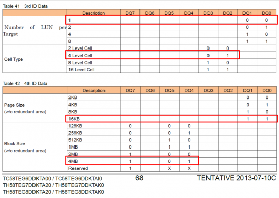
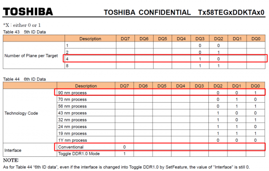
I don't find the datasheet for this NAND but I find some characteristics from the "TC58TEG6DDKTA00-Toshiba" datasheets.
Attachment:
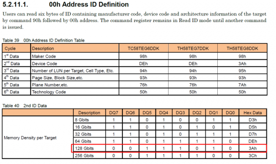 id1.png [ 159.83 KiB | Viewed 12266 times ]
Attachment:
 id2.png [ 122.63 KiB | Viewed 12266 times ]
Attachment:
 id3.png [ 121.96 KiB | Viewed 12266 times ]
Here is the supposed caraceristics of the NAND Flash
Code:
#define NAND_SIZE_KB (16*1024*1024) // 16777216 KB
#define BLOC_SIZE_KB (4*1024) // 4096 KB
#define BLOC_SIZE_BYTE (BLOC_SIZE_KB*1024) // 4194304 B
#define PAGE_SIZE_KB (16) // 16 KB
#define PAGE_SIZE_BYTE (PAGE_SIZE_KB*1024) // 16384 B
#define BLOC_COUNT (NAND_SIZE_KB/BLOC_SIZE_KB) // 4096 BLOCKS
#define PAGE_PER_BLOC (BLOC_SIZE_KB/PAGE_SIZE_KB) // 256 PAGES

