All times are UTC - 5 hours [ DST ]


Post new topic Reply to topic  [ 11 posts ] 
Author Message
 Post subject: WD SN520 Nvme
PostPosted: March 2nd, 2023, 9:07 
Offline

Joined: September 9th, 2020, 8:51
Posts: 12
Location: italy
Hi everyone, I have this SSD that is not being detected. After trying a few measurements, there doesn't seem to be any short circuits. Does anyone have any suggestions? Are there any pins to try to put it in safe mode?

Thanks in advance


Attachments:
20230302_140050.jpg
20230302_140050.jpg [ 1.57 MiB | Viewed 3257 times ]
Top
 Profile  
 
 Post subject: Re: WD SN520 Nvme
PostPosted: March 2nd, 2023, 13:25 
Offline
User avatar

Joined: September 8th, 2009, 18:21
Posts: 15528
Location: Australia
FWIW, some SanDisk SSDs use the NAND Ready/Busy* pin as the ROM mode jumper.

_________________
A backup a day keeps DR away.


Top
 Profile  
 
 Post subject: Re: WD SN520 Nvme
PostPosted: March 2nd, 2023, 13:59 
Offline
User avatar

Joined: September 8th, 2009, 18:21
Posts: 15528
Location: Australia
The tiny BGA device near the ACT9045VM333 PMIC is a load switch. Check the input and output voltages.

NCP451FCT2G, ON Semiconductor, load switch, 0.75V – 5.5Vin, 3A, 13mOhm Rdson, marking 451, WLCSP6

NCP451AFCT2G, Onsemi, Load Switch, 3A, 0.75V - 5.5Vin, marking 51A, WLCSP6

https://www.onsemi.com/download/data-sheet/pdf/ncp451-d.pdf

_________________
A backup a day keeps DR away.


Top
 Profile  
 
 Post subject: Re: WD SN520 Nvme
PostPosted: March 3rd, 2023, 6:12 
Offline

Joined: September 9th, 2020, 8:51
Posts: 12
Location: italy
Hi,

thanks for your reply.
It's not easy to take the measurement, but it appears to be input 0.110V output 3.3V.

Thanks


Top
 Profile  
 
 Post subject: Re: WD SN520 Nvme
PostPosted: March 3rd, 2023, 6:25 
Offline

Joined: November 7th, 2020, 5:31
Posts: 1091
Location: The_UK
n3dv3d wrote:
It's not easy to take the measurement, but it appears to be input 0.110V output 3.3V.
Are you sure you haven't reversed vin and vout :wink:

_________________
Data Recovery Services in the UK.
https://www.usbrecovery.co.uk/


Top
 Profile  
 
 Post subject: Re: WD SN520 Nvme
PostPosted: March 3rd, 2023, 6:56 
Offline

Joined: September 9th, 2020, 8:51
Posts: 12
Location: italy
Lardman wrote:
n3dv3d wrote:
It's not easy to take the measurement, but it appears to be input 0.110V output 3.3V.
Are you sure you haven't reversed vin and vout :wink:


sound strange to me too but:


Attachments:
tempsnip.png
tempsnip.png [ 16.85 KiB | Viewed 3119 times ]
Top
 Profile  
 
 Post subject: Re: WD SN520 Nvme
PostPosted: March 3rd, 2023, 10:42 
Offline

Joined: November 7th, 2020, 5:31
Posts: 1091
Location: The_UK
Where are you taking the measurements - can you measure resistance to ground pins c1 and c2.

_________________
Data Recovery Services in the UK.
https://www.usbrecovery.co.uk/


Top
 Profile  
 
 Post subject: Re: WD SN520 Nvme
PostPosted: March 3rd, 2023, 10:59 
Offline

Joined: September 9th, 2020, 8:51
Posts: 12
Location: italy
Lardman wrote:
Where are you taking the measurements - can you measure resistance to ground pins c1 and c2.


I measured voltage between A1<->GND and A2<->GND.
Resistence C1<->C2 seems to be about 1,9Mohm.

Thanks


Top
 Profile  
 
 Post subject: Re: WD SN520 Nvme
PostPosted: March 3rd, 2023, 12:28 
Offline

Joined: November 7th, 2020, 5:31
Posts: 1091
Location: The_UK
What was their resistance to ground not to each other, it will confirm your chip orientation.

_________________
Data Recovery Services in the UK.
https://www.usbrecovery.co.uk/


Top
 Profile  
 
 Post subject: Re: WD SN520 Nvme
PostPosted: March 3rd, 2023, 12:33 
Offline
User avatar

Joined: September 8th, 2009, 18:21
Posts: 15528
Location: Australia
I'm basing my identification of the load switch on other photos. Have I correctly identified the marking?

_________________
A backup a day keeps DR away.


Top
 Profile  
 
 Post subject: Re: WD SN520 Nvme
PostPosted: March 3rd, 2023, 17:59 
Offline
User avatar

Joined: September 8th, 2009, 18:21
Posts: 15528
Location: Australia
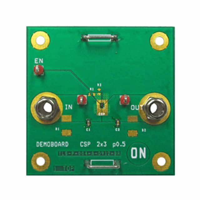
The demo board on page 8 of the datasheet shows that the pins are reversed. It looks like the top view is actually a bottom view.

This demo PCB seems to confirm the error:

https://media.digikey.com/Photos/On%20Semi%20Photos/MFG_NCP451FCT2GEVB.jpg

Can you measure any voltages at the inductors and capacitors surrounding the ACT9045VM333 PMIC? If not, check that the output of the load switch is not shorted to ground. Also confirm that there are no shorts to ground around the PMIC.

If all is good, then you should be able to bridge Vin and Vout at the load switch.


Edit: Confirm that the load switch is being enabled. There may be a missing control input from the DevSleep pin on the interface (DevSleep should be 0V).

_________________
A backup a day keeps DR away.


Top
 Profile  
 
Display posts from previous:  Sort by  
Post new topic Reply to topic  [ 11 posts ] 

All times are UTC - 5 hours [ DST ]


Who is online

Users browsing this forum: No registered users and 24 guests


You cannot post new topics in this forum
You cannot reply to topics in this forum
You cannot edit your posts in this forum
You cannot delete your posts in this forum
You cannot post attachments in this forum

Search for:
Jump to:  
Powered by phpBB © 2000, 2002, 2005, 2007 phpBB Group