OCZ Vertex 450 schematic
May 3rd, 2024, 6:39
Hi All !
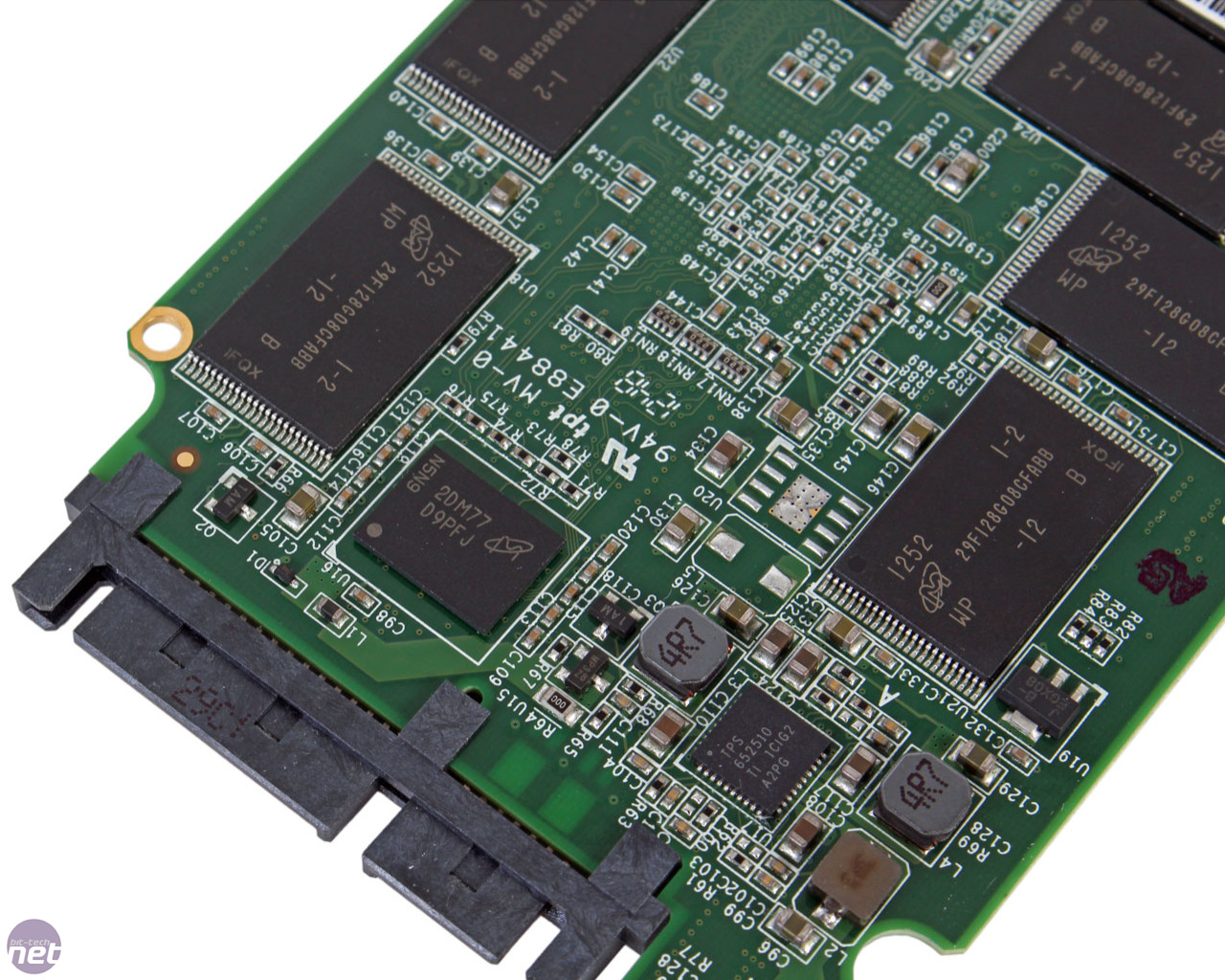
My ancient SSD burned out. I want to restore information. I found a capacitor that is heating up a lot, but I don't know what to replace it with. C105. Thanks in advance for your suggestions.
My ancient SSD burned out. I want to restore information. I found a capacitor that is heating up a lot, but I don't know what to replace it with. C105. Thanks in advance for your suggestions.
- Attachments
-
Re: OCZ Vertex 450 schematic
May 3rd, 2024, 11:53
Remove it and run the SSD without it.
Re: OCZ Vertex 450 schematic
May 3rd, 2024, 12:19
Do you think it is just filter, 1uF ?
Re: OCZ Vertex 450 schematic
May 3rd, 2024, 13:26
There doesn't appear to be any DC-DC converter on the other side of the PCB, so I think it's probably a filter.
Re: OCZ Vertex 450 schematic
May 3rd, 2024, 13:28
I measured it with a tester. The capacitor behaves as it should. First it shows low resistance, then it shows infinity. I don't understand how it can be hot. Only if there is AC going through it 
Re: OCZ Vertex 450 schematic
May 3rd, 2024, 14:24
The resistance between +5 and ground is about 80ohm. I don't think it should be like that.
Re: OCZ Vertex 450 schematic
May 3rd, 2024, 14:32
If that capacitor is responsible for the 80 ohms reading, then that's not enough to shut down the 5V supply. This means that the real problem is elsewhere. Your capacitor is then a secondary, non-fatal problem.
I would measure the outputs of the DC-DC converters. If these are OK, then the firmware has probably "panicked" due to bad NAND.
I this model has a UART port that provides diagnostic output.
I would measure the outputs of the DC-DC converters. If these are OK, then the firmware has probably "panicked" due to bad NAND.
I this model has a UART port that provides diagnostic output.
Re: OCZ Vertex 450 schematic
May 4th, 2024, 5:33
How to understand where to measure DC ? Do you think inductors like L1 and so on can be good points ?
- Attachments
-
-
Re: OCZ Vertex 450 schematic
May 4th, 2024, 14:03
Measure the voltages at L2, L3, L4 adjacent to U17 (TPS652510).
https://www.ti.com/lit/ds/symlink/tps652510.pdf
I can't identify the markings on U19, but I suspect that this is an LDO regulator.
https://www.ti.com/lit/ds/symlink/tps652510.pdf
I can't identify the markings on U19, but I suspect that this is an LDO regulator.
Re: OCZ Vertex 450 schematic
May 4th, 2024, 15:58
U19 is RT9166-25PXL.
RT9166-25PXL, Richtek, 2.5V 0.3A Ultra-Fast Transient Response LDO Regulator, marking JB-, SOT89:
https://www.richtek.com/assets/product_file/RT9166=RT9166A/DS9166A-24.pdf
https://images.bit-tech.net/content_images/2013/09/ocz-vertex-450-256gb-review/vertex450-7b.jpg
RT9166-25PXL, Richtek, 2.5V 0.3A Ultra-Fast Transient Response LDO Regulator, marking JB-, SOT89:
https://www.richtek.com/assets/product_file/RT9166=RT9166A/DS9166A-24.pdf
https://images.bit-tech.net/content_images/2013/09/ocz-vertex-450-256gb-review/vertex450-7b.jpg
Re: OCZ Vertex 450 schematic
May 6th, 2024, 15:23
L3 - 0
and see pictures. I have tried to find more as 5V, but not.
and see pictures. I have tried to find more as 5V, but not.
- Attachments
-
-
Re: OCZ Vertex 450 schematic
May 6th, 2024, 15:54
Measure the resistance between L3 and ground (any screw hole). If this is shorted, then hopefully it will be due to a shorted capacitor. The missing voltage at this point appears to be ~3V, which is the Vcc for the NAND flash array.
BTW, I don't understand why you are seeing 4V instead of 5V at those test points. ?
?
BTW, I don't understand why you are seeing 4V instead of 5V at those test points.
Re: OCZ Vertex 450 schematic
May 6th, 2024, 16:10
As you see input is 5V, but on LDO is 4V. Seems some element is draining 1V.
According PDF :
Buck1 = 1.2 V Buck2 = 1.8 V Buck3 = 3.3 V
According PDF :
Buck1 = 1.2 V Buck2 = 1.8 V Buck3 = 3.3 V
Re: OCZ Vertex 450 schematic
May 6th, 2024, 16:37
have not found 0R on L and capacitors. But voltage is less as expected in many points.
See pic.
See pic.
- Attachments
-
Re: OCZ Vertex 450 schematic
May 6th, 2024, 17:40
Check R64 (near L3).
Re: OCZ Vertex 450 schematic
May 6th, 2024, 18:14
R64 - 0 as expected.
I tested very carefully all capacitors. Except this list all of them as expected:
C55 - 75 Ohm
C129, C184, C155, C146 - around 90 Ohm.
I tested very carefully all capacitors. Except this list all of them as expected:
C55 - 75 Ohm
C129, C184, C155, C146 - around 90 Ohm.
Re: OCZ Vertex 450 schematic
May 6th, 2024, 18:38
Maybe I was wrong about the screw holes. Instead, I would use SATA power ground as the 0V reference.
There is a small inductor, L1, in series with the 5V supply.
A resistance of ~100 ohms is normal for the Vcore supply for the flash controller.
What is the resistance between the Vin pins of the LDO regular, DC-DC converter and SATA 5V?
Check the ENable pin for the 3.3V converter.
There is a small inductor, L1, in series with the 5V supply.
A resistance of ~100 ohms is normal for the Vcore supply for the flash controller.
What is the resistance between the Vin pins of the LDO regular, DC-DC converter and SATA 5V?
Check the ENable pin for the 3.3V converter.
Re: OCZ Vertex 450 schematic
May 7th, 2024, 15:20
Thanks a lot. You are wizard Resistance was higher as expected to have on L1, I replaced it to any I have and just see picture.
Now all measures are 5V, where before were 4V.
Now all measures are 5V, where before were 4V.
- Attachments
-
Re: OCZ Vertex 450 schematic
May 7th, 2024, 16:14
It appears that the failure of C105 may have stressed L1.
Re: OCZ Vertex 450 schematic
May 8th, 2024, 6:26
Maybe this topic will help someone else to repair OCZ Vertex 450.
Powered by phpBB © phpBB Group.