Motivated by the research above, I thought I might test out my JTagulator on an SD card.
This particular card is a 2GB Sony Class 4. The controller appears to be made by Phison, a PS2233 or something close. The NAND ID is 0x98 0xD5 0x94 0x32 and the part number is likely HVPE4F4. I have seen the manufacturer of these to be listed in vatious places as both Toshiba and Hynix, and also Samsung. I don't know which it is.
Attachment:
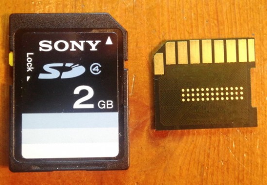 1.jpg [ 106.6 KiB | Viewed 7678 times ]
Attachment:
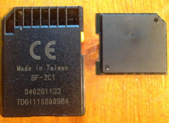 2.jpg [ 113.03 KiB | Viewed 7678 times ]
I noticed that after the coating was removed, there were 2 sets of traces leading to the edge of the card. I was thinking test point or programming points.
Attachment:
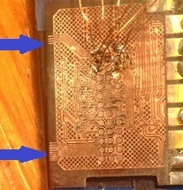 3.jpg [ 35.02 KiB | Viewed 7678 times ]
Attachment:
 traces.jpg [ 60.89 KiB | Viewed 7678 times ]
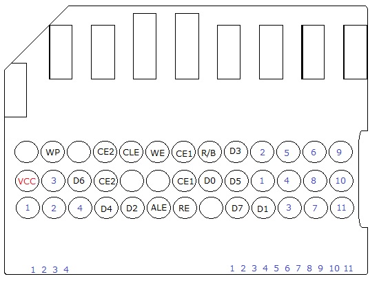
I decided to start with the smaller set, 4 traces. I soldered some thin wires under the microscope to the pads that were not used for the NAND Flash chip.
Attachment:
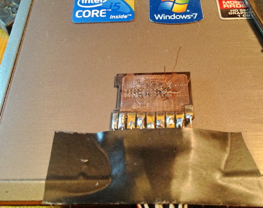 3a.jpg [ 101.18 KiB | Viewed 7678 times ]
The wires were too fragile so I made up a board to hold it, and also extension made from a sd-microsd adapter so I could insert it in my laptop still while analysing.
Attachment:
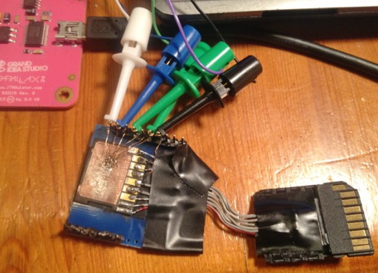 4.jpg [ 135.55 KiB | Viewed 7678 times ]
Here is the whole setup.
Attachment:
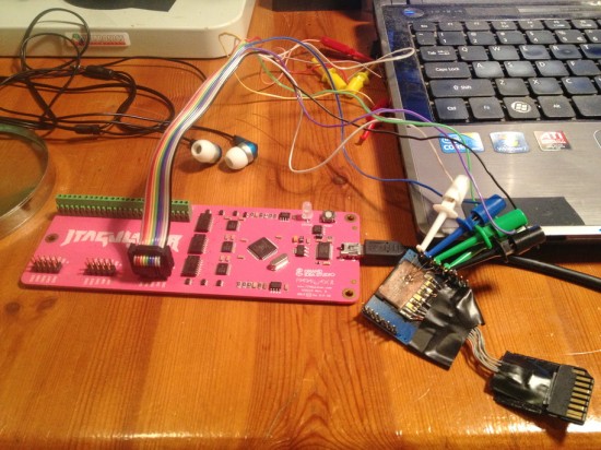 5.jpg [ 291.46 KiB | Viewed 7678 times ]
I will post details of what signals I find soon, I didn't realise the time until the birds started singing.. dang, another day feeling tired coming up